- 您现在的位置:买卖IC网 > Sheet目录3882 > PIC16F87T-E/ML (Microchip Technology)IC MCU FLASH 4KX14 EEPROM 28QFN
LC88F83B0A
No.A1228-17/25
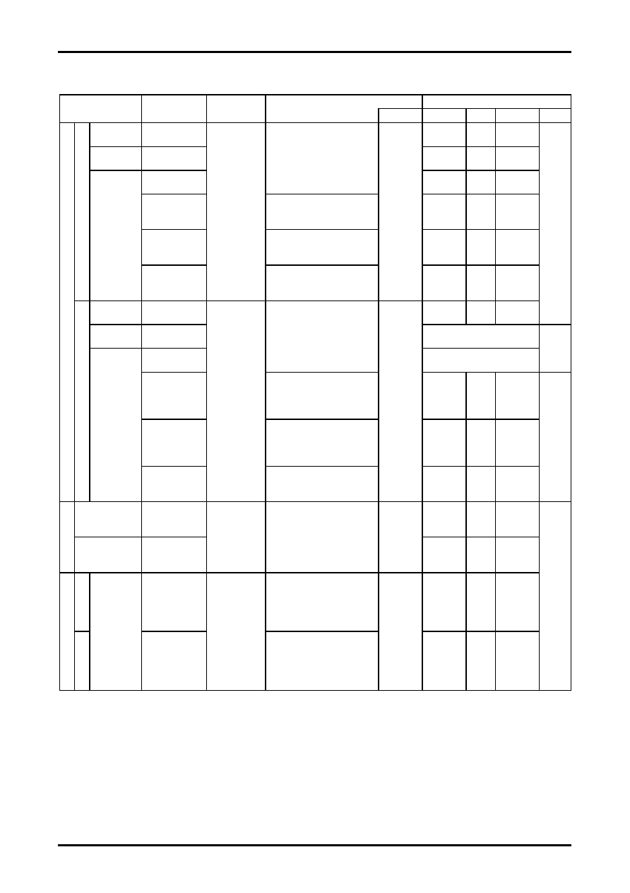
Serial I/O Characteristics at Ta = -20°C to +75°C, VSS = LCDVSS0 = LCDVSS1 = 0V
1. SIO0 Serial I/O Characteristics (Wake-up function is not in use) (Note 4-1-1)
Parameter
Symbol
Pin/Remarks
Conditions
Specification
VDD[V]
min
typ
max
unit
Serial
c
lock
Inpu
tclo
c
k
Frequency
tSCK(1)
SCK0(P12)
See Fig. 6.
2.3 to 5.5
4
tCYC
Low level
pulse width
tSCKL(1)
2
High level
pulse width
tSCKH(1)
2
tSCKHA(1)
Automatic communication
mode
See Fig. 6.
6
tSCKHBSY(1a)
Automatic communication
mode
See Fig. 6.
23
tSCKHBSY(1b)
Excluding Automatic
communication mode
See Fig. 6.
4
Out
p
ut
c
lock
Frequency
tSCK(2)
SCK0(P12)
CMOS output selected
See Fig. 6.
2.3 to 5.5
4
Low level
pulse width
tSCKL(2)
1/2
tSCK
High level
pulse width
tSCKH(2)
1/2
tSCKHA(2)
Automatic communication
mode
CMOS output selected
See Fig. 6.
6
tCYC
tSCKHBSY(2a)
Automatic communication
mode
CMOS output selected
See Fig. 6.
4
23
tSCKHBSY(2b)
Excluding automatic
communication mode
See Fig. 6.
4
Serial
i
nput
Data setup time
tsDI(1)
SI0(P11),
SB0(P11)
Must be specified with respect
to rising edge of SIOCLK.
See Fig. 6.
2.3 to 5.5
0.03
μs
Data hold time
thDI(1)
0.03
S
e
ri
a
lou
tp
ut
Inpu
tclo
c
k
Output
delay time
tdD0(1)
SO0(P10),
SB0(P11)
(Note4-1-2)
2.3 to 5.5
1tCYC
+0.05
Out
p
ut
c
lock
tdDO(2)
(Note4-1-2)
1tCYC
+0.05
Note 4-1-1: These specifications are theoretical values. Add margin depending on its use.
Note 4-1-2: Must be specified with respect to falling edge of SIOCLK. Must be specified as the time to the beginning of
output state change in open drain output mode. See Fig.6.
发布紧急采购,3分钟左右您将得到回复。
相关PDF资料
PIC16F87-E/ML
IC MCU FLASH 4KX14 EEPROM 28QFN
PIC18LF4320-I/ML
IC MCU FLASH 4KX16 EEPROM 44QFN
PIC16F77T-I/PTG
IC MCU FLASH 8KX14 W/AD 44TQFP
PIC16LF1933-I/SO
IC PIC MCU FLASH 4K 28-SOIC
PIC16C54C-20I/SO
IC MCU OTP 512X12 18SOIC
PIC16LF726-I/SO
IC PIC MCU FLASH 8K 1.8V 28-SOIC
PIC12CE673-10/P
IC MCU OTP 1KX14 A/D&EE 8DIP
PIC16F726-I/SO
IC PIC MCU FLASH 8KX14 28-SOIC
相关代理商/技术参数
PIC16F87T-E/SO
功能描述:8位微控制器 -MCU 20MHz 4K Flash RoHS:否 制造商:Silicon Labs 核心:8051 处理器系列:C8051F39x 数据总线宽度:8 bit 最大时钟频率:50 MHz 程序存储器大小:16 KB 数据 RAM 大小:1 KB 片上 ADC:Yes 工作电源电压:1.8 V to 3.6 V 工作温度范围:- 40 C to + 105 C 封装 / 箱体:QFN-20 安装风格:SMD/SMT
PIC16F87T-E/SS
功能描述:8位微控制器 -MCU 20MHz 4K Flash RoHS:否 制造商:Silicon Labs 核心:8051 处理器系列:C8051F39x 数据总线宽度:8 bit 最大时钟频率:50 MHz 程序存储器大小:16 KB 数据 RAM 大小:1 KB 片上 ADC:Yes 工作电源电压:1.8 V to 3.6 V 工作温度范围:- 40 C to + 105 C 封装 / 箱体:QFN-20 安装风格:SMD/SMT
PIC16F87T-I/ML
功能描述:8位微控制器 -MCU 7KB 368 RAM 16 I/O RoHS:否 制造商:Silicon Labs 核心:8051 处理器系列:C8051F39x 数据总线宽度:8 bit 最大时钟频率:50 MHz 程序存储器大小:16 KB 数据 RAM 大小:1 KB 片上 ADC:Yes 工作电源电压:1.8 V to 3.6 V 工作温度范围:- 40 C to + 105 C 封装 / 箱体:QFN-20 安装风格:SMD/SMT
PIC16F87T-I/SO
功能描述:8位微控制器 -MCU 7KB 368 RAM 16 I/O RoHS:否 制造商:Silicon Labs 核心:8051 处理器系列:C8051F39x 数据总线宽度:8 bit 最大时钟频率:50 MHz 程序存储器大小:16 KB 数据 RAM 大小:1 KB 片上 ADC:Yes 工作电源电压:1.8 V to 3.6 V 工作温度范围:- 40 C to + 105 C 封装 / 箱体:QFN-20 安装风格:SMD/SMT
PIC16F87T-I/SS
功能描述:8位微控制器 -MCU 7KB 368 RAM 16 I/O RoHS:否 制造商:Silicon Labs 核心:8051 处理器系列:C8051F39x 数据总线宽度:8 bit 最大时钟频率:50 MHz 程序存储器大小:16 KB 数据 RAM 大小:1 KB 片上 ADC:Yes 工作电源电压:1.8 V to 3.6 V 工作温度范围:- 40 C to + 105 C 封装 / 箱体:QFN-20 安装风格:SMD/SMT
PIC16F882-E/ML
功能描述:8位微控制器 -MCU 3.5KB Enh FLSH 128 RAM RoHS:否 制造商:Silicon Labs 核心:8051 处理器系列:C8051F39x 数据总线宽度:8 bit 最大时钟频率:50 MHz 程序存储器大小:16 KB 数据 RAM 大小:1 KB 片上 ADC:Yes 工作电源电压:1.8 V to 3.6 V 工作温度范围:- 40 C to + 105 C 封装 / 箱体:QFN-20 安装风格:SMD/SMT
PIC16F882-E/SO
功能描述:8位微控制器 -MCU 3.5KB Enh FLSH 128 RAM RoHS:否 制造商:Silicon Labs 核心:8051 处理器系列:C8051F39x 数据总线宽度:8 bit 最大时钟频率:50 MHz 程序存储器大小:16 KB 数据 RAM 大小:1 KB 片上 ADC:Yes 工作电源电压:1.8 V to 3.6 V 工作温度范围:- 40 C to + 105 C 封装 / 箱体:QFN-20 安装风格:SMD/SMT
PIC16F882-E/SP
功能描述:8位微控制器 -MCU 3.5KB Enh FLSH 128 RAM RoHS:否 制造商:Silicon Labs 核心:8051 处理器系列:C8051F39x 数据总线宽度:8 bit 最大时钟频率:50 MHz 程序存储器大小:16 KB 数据 RAM 大小:1 KB 片上 ADC:Yes 工作电源电压:1.8 V to 3.6 V 工作温度范围:- 40 C to + 105 C 封装 / 箱体:QFN-20 安装风格:SMD/SMT